
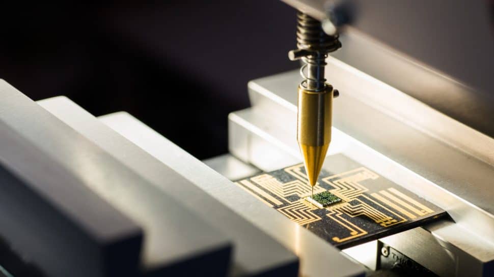
As part of the LDS process, a laser is used to create a conductive trace on the injection-molded plastic component itself.
A unique LDS additive is included into the injection-moulded plastic. Injection moulding is the initial step in the process of creating the final product. The laser beam then activates the additive by exposing the places where conductor structures will subsequently be located. It’s during this copper bath metallization that the active portions of the surface develop conductive traces with strong adherence and crisp shapes. Nickel and gold, silver, or soldering tin, for example, may be built up in this manner in consecutive layers.
It’s been proven many times over.
There are several common uses for the LDS technology. Pressure sensors, for example, are an example of a small sensor. LDS-based MIDs are also seen in mobile phones. These three-dimensional moulded connection devices are used in millions of phones as antennas that save space. There are a variety of other uses for this technology in fields such as medicine, air conditioning, and security in teprosa.
Plating in through-holes
MID surface connection may be made using LPKF LDS technology’s plated-through holes, which are dependable. This increases the layout options.
- WeL DS: 3D-MIDs and laser plastic welding in one unique package.
Laser plastic welding and 3D-MIDs are combined in WeLDS. Injection moulded items may have conductive pathways etched into them using LDS. In addition, LPKF’s laser plastic welding guarantees aesthetically and operationally exceptional weld seams for long-lasting and dependable connections of LDS parts. Thus, the method provides revolutionary prospects for further downsizing and functional integration in the teprosa electronic sector.
- 3D LDS components may be effectively sealed and protected.
- LDS components have a higher geometrical complexity.
- Production at a profit
- Integration of many functions at a high level
The new technology
Three-dimensional mechanical and electronic integration (or 3D-MID) is a multidisciplinary technique. Moulded injection moulded plastic substrates serve as carriers for 3D circuitry and electronic devices together with connection items including connectors, cable assemblies and flexible circuit lines for 3D-MID components.
In order to produce 3D-MID items teprosa, there are a variety of methods. For creating the circuit on the substrate, the LDS technique of LPKF (Laser Direct Structuring) is now the most used method. After moulding the 3D substrate, an IR laser beam with a spot width of 50 to 100 micrometres is used to build the 3D circuitry on the substrate. Finishing layers such as nickel, gold, or silver may be applied to the structured region after the copper solution has been plated. Pick and place machines are then used to assemble the electrical components. For example, the 3D-MID substrate is connected to other components by means of various assembly techniques like as soldering and bonding.
Areas of application
As a result, 3D-MID has a wide range of applications in both present and future technology. 3D-MID may be used in a wide variety of ways:
- Sensors \Switches
- Antennas
- Carriers for LEDs
- components for lighting in a building
- Connectors and modules for connection
- 3D circuits in electrical packaging that is very small
- Intruder detection and prevention systems
Lasers with ultra-short pulses are increasingly used in current material processing applications.
Modern material processing relies heavily on ultra-short pulse lasers. Many systems that use ultra-short pulse lasers may be used for a variety of tasks such as cutting, engraving, or marking. It is now possible to process materials more effectively thanks to these new lasers. A pico- or femto-laser may be used to shape any material, including plastics, metals, glass, and diamonds.